Notes about DRAM components
本文将mark下DRAM components相关notes。
Basic
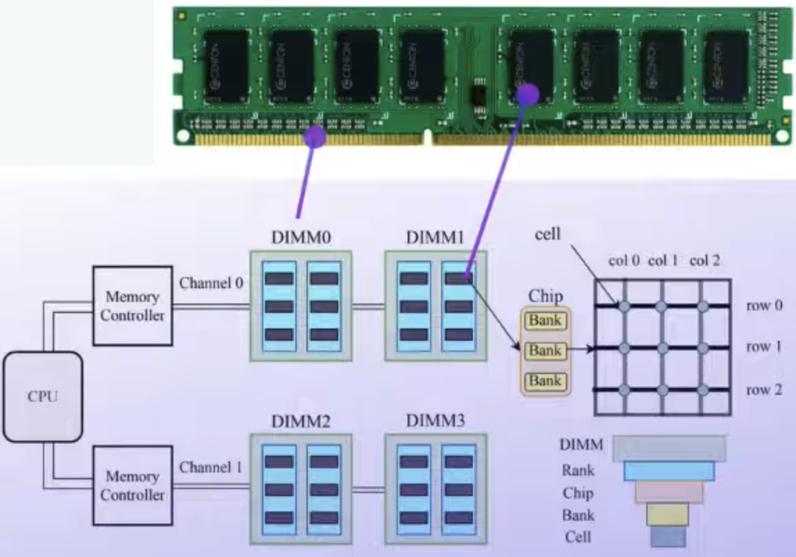
In modern cloud servers, a CPU(socket) has several memory controllers. Each controller communicates with DIMMs through high-speed memory channels. Usually, a memory channel is shared by several DIMM slots. A DIMM has several ranks, and each is composed of sevaral DRAM chips. For typical DDR4 DIMMs, a rank is composed of 16 chips for data bits and 2 additional chips for ECC bits. A chip consists of multiple banks, which enables the access parallesim. A DRAM bank is structured as a two-dimensional cell array indexed by rows and columns.
- socket
- memory controller
- channel
- DIMM(Dual In-Line Memory Module)
- rank
- chip
- bank
- cell (row, column)
DQ pin
DQ pin 是 DRAM 芯片和内存控制器之间传输数据的“数据引脚”(Data pin)。
可以把它理解成内存芯片对外的数据线接口。
CPU 不直接连接 DRAM cell,路径大概是:
1 | CPU / Memory Controller |
CPU 想读数据:
1 | DRAM内部cell |
写数据则相反:
1 | Memory Controller |
x4/x8/x16 device width
简单理解:
1 | x4 DRAM chip |
1 | x8 DRAM chip |
1 | x16 DRAM chip |
一个 Rank 为什么有很多 DRAM 芯片?
因为一个 DRAM 芯片的数据宽度太小。
例如 DDR4 RDIMM的配置:
1 | 一个 Rank: |
画一下:
1 | 一个 Rank |
总数据宽度:
1 | 18 × 4 bit |
其中:
1 | 64 bit 数据 |
所以服务器内存常见:
1 | 64-bit data + ECC |
就是这样来的。
DQ lane
简单理解:
1 | 一个 x4 DRAM: |
所以:
1 | DQ pin: |
关系:
1 | Lane |
参考资料: