Notes about F-NIC(FPGA-based SmartNIC)
本文将mark下F-NIC(FPGA-based SmartNIC)相关notes。
We describe bump-in-the-wire(是一种网络技术概念,指在网络通信链路中透明插入的设备或系统,用于增强特定功能而不改变终端设备的配置或通信协议) F-NICs, focusing on Mellanox Innova.
Bump-in-the-wire
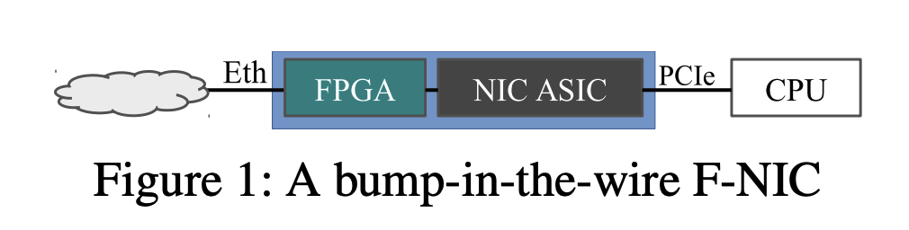
A typical F-NIC (Figure 1) combines a commodity network ASIC (e.g., ConnectX-4 Lx NIC) with an FPGA and local DRAM. The FPGA is located between the ASIC and the network port, interposing on all Ethernet traffic in and out of the NIC. The FPGA and the ASIC communicate directly via an internal bus (e.g., 40 Gbps Ethernet), and a PCIe bus connects the ASIC to the host.
The bump-in-the-wire design reuses the existing data and control planes between the CPU and the NIC ASIC, with its QoS management, and virtualization support (SR-IOV), mature DMA engines, and software stack.
F-NIC programming
The development of an F-NIC accelerated application involves both hardware logic on FPGA and associated software on the CPU. F-NIC vendors provide a lightweight shell IP: a set of low-level hardware interfaces for basic operations, including link-layer packet exchange with the network and the host, onboard DRAM access, and control register access. However, the vendor SDK leaves it to customers to implement higher level features such as FPGA network stack processing or virtualization support.
参考资料: